
X-Meritan is a professional China quality Slices with Diffusion Barriers supplier. The thin sheet with a diffusion barrier layer is a cost-effective solution developed by X-Meritan to enhance the welding reliability of Peltier modules. It addresses the problem of solder penetration during the high-temperature packaging of semiconductor materials. By integrating Nickel Diffusion Barrier for Bi2Te3 Slices on the extrusion die, we have achieved high-precision customization with a thickness starting from 0.3 millimeters and a cutting accuracy within ±15 micrometers. This provides high-performance pre-processing materials for global system integrators.
The quality Slices with Diffusion Barriers by X-Meritan can play a role of a quality guardian in advanced semiconductor thermal management. The core of this lies in preventing the solder components from penetrating the semiconductor substrate during long-term thermal cycling, which would lead to performance degradation. As a Multi-layer Metallized Slices with Diffusion Barriers, it adopts a proprietary nickel-based alloy technology and offers various solderable layer options such as tin electroplating or chemical gold plating. This Electroless Nickel Plating Slices with Diffusion Barriers not only effectively resists oxidation but also demonstrates extremely high physical stability in extreme high-temperature or strong cycling environments thanks to the patented "H" technology.
A semiconductor wafer with a diffusion barrier layer is a special semiconductor component, usually having a nickel base layer, designed to prevent solder penetration and damage to the semiconductor material. These barriers function as protective film interfaces, which can prevent the mutual diffusion (mixing) between semiconductor materials, such as preventing metal interconnections from reacting or diffusing into silicon, thereby ensuring the structural and electrical integrity of the device.
| Key Feature | Technical Specifications | Customer Value |
| Base Material | Extruded Bi2Te3-Sb2Te3 Ingots | Provides extremely high mechanical strength and thermoelectric consistency. |
| Wafer Thickness | >= 0.3 mm (Customizable per drawing) | Supports the development of miniaturized and ultra-thin TEC components. |
| Cutting Precision | +/- 15 microns | Reduces end-face tilting during packaging; improves final product yield. |
| Electroless Tin Plating | 7 microns +/- 2 microns | Excellent solder affinity; effectively extends storage and shelf life. |
| Electroless Gold Plating | < 0.2 microns (Au) | Excellent conductivity and anti-oxidation; ideal for Gold-Tin (AuSn) soldering. |
| Patented "H" Tech | ~150 micron Aluminum (Al) barrier | Designed for extreme conditions like aerospace or heavy industrial cycling. |
By superimposing multiple layers of metallization technology on the nickel diffusion barrier layer of Bi2Te3 block-shaped materials, our Slices with Diffusion Barriers can form a dense barrier. This effectively prevents the diffusion of low-melting-point solder atoms such as tin (Sn) into the thermoelectric material, thereby avoiding module failure caused by resistance deviation.
For scenarios such as aerospace or precision medical PCR that require frequent switching between cold and hot modes, we recommend the patented "H technology". This solution incorporates a thick aluminum layer of up to 150 micrometers within multiple barrier layers, which can significantly mitigate thermal stress and ensure that multi-layer metallized block materials with diffusion barrier layers do not separate or crack under high-intensity cycles.
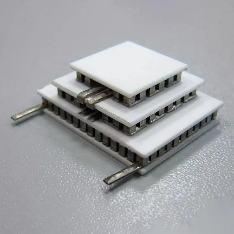
For TEC factories that cannot perform slicing themselves, we offer turnkey services. Each piece of chemically plated nickel block material with a diffusion barrier layer undergoes precise grinding and cutting to ensure that the thickness tolerance is controlled within an extremely narrow range, enabling downstream automatic lamination machines to achieve efficient and stable electrochemical pair grasping.
Q: Why is our Slices with Diffusion Barriers more suitable for high-temperature welding?
A: Because we have adopted a special multi-layer electroplating technology using nickel-based alloys instead of a single nickel plating. This structure can maintain the chemical stability of the interface even under the temperature fluctuations of reflow soldering, ensuring the formation of extremely strong intermetallic compounds (IMC) between the sheet and the solder.
Q: How should one choose between tin plating and gold plating?
A: Tin electroplating (7 microns) is more suitable for conventional lead-tin or lead-free solder paste processes and offers extremely high cost-effectiveness. While chemical gold plating (< 0.2 microns) is mainly recommended for precision optical communication module manufacturing scenarios where high stability of resistance is required, or for the use of gold-tin (AuSn) solder.
As a professional manufacturer of electric heating materials in China, X-Meritan has its own factory and, with its fluent English communication skills and solid technical background, has gained the trust of customers worldwide. Currently, our product presence has extended to markets all over the world, including Europe, South America, and Southeast Asia.